.png?width=400&height=150&name=Untitled%20design%20(56).png)

As a civil engineering student, I had the opportunity to explore various branches of engineering, including electrical engineering. During this journey, I was introduced to printed circuit board (PCB) design, and I was fascinated by the process of creating circuits and understanding how each component works together to form a functional design.
I quickly learned that choosing the best PCB design software is crucial to ensuring efficient, reliable, and high-quality designs. The right software streamlines the design process, provides robust tools for routing, simulating, and validating circuits, and helps manage complexity while ensuring the final product meets all technical requirements.
Fast-forward to today, I’ve evaluated a wide range of PCB design software tools to evaluate their performance, usability, and features. With numerous options available, it was essential for me to delve into each tool's capabilities and assess how they handle real-world projects.
By blending expert opinion with valuable feedback from G2 users, I’ve compiled a list of the 7 best PCB design software to help you find the best fit for your own projects.
Altium Designer: Best for advanced design tools and an extensive component library
Offers powerful layout and schematic tools for professional PCB design. ($355/month)
Altium 365: Best for PCB layout editing and 3D visualization
Enables collaborative design with cloud-based 3D visualization. (cost depends on the connectors chosen)
PADS Professional: Best for complex PCB layouts and advanced routing
Handles high-density designs with precision routing capabilities. ($286.92/month)
Allegro PCB Designer: Best for high-density designs and error correction
Provides robust tools for managing large-scale, complex PCBs. (pricing available on request)
Autodesk Fusion: Best for integrated mechanical and electrical design
Combines PCB design with 3D modeling and mechanical integration ($85/month)
Altium CircuitMaker: Best community-driven, open-source PCB design tool
Free platform that fosters collaboration among hobbyists and professionals. (free)
Autodesk EAGLE: Best for intuitive interface and schematic capture
Simplifies PCB design with user-friendly schematic and layout tools. (pricing available on request)
* These PCB design software are top-rated in their category, according to G2's 2025 Winter Grid Report. I’ve also added their monthly pricing to make comparisons easier for you.
PCB design software is a powerful tool used to create and optimize printed circuit board layouts. It helps engineers design the electronic circuits that form the backbone of modern devices.
As I explored the best PCB design software, I found that they offer more than basic layout capabilities. They provide advanced features like real-time collaboration, 3D visualization, and error-checking. The global PCB design software market is projected to grow from $4.12 billion in 2025 to $13.32 billion by 2034, reflecting a robust demand for these tools
Evaluating various tools with professionals on small projects allowed me to identify features that improved the design process while also helping me relive my engineering days. In this article, I’ll highlight what made these tools stand out and how they helped me overcome common design challenges.
I started by reviewing G2’s latest Grid Reports to identify which PCB design software platforms consistently excel in usability, feature completeness, and overall satisfaction. This gave me a strong baseline of trusted tools that electrical engineers already rely on.
From there, I narrowed my list by getting hands-on experience with the features and workflows. For solutions where direct testing wasn’t fully possible, I leaned on verified G2 user feedback, product demos, and vendor documentation to understand real-world performance and limitations. I also used AI-powered analysis to scan thousands of user reviews, surfacing common praise points and recurring frustrations.
Throughout testing, I focused on the experience from an engineer’s perspective: Was the platform intuitive? Did it simplify PCB layout, optimization, and management? Could it handle complex designs without a steep learning curve? And most importantly, would it integrate smoothly into existing engineering workflows?
Screenshots in this article combine my testing visuals with verified vendor images from G2.
When evaluating PCB design tools, I consider features that streamline the design process, enhance efficiency, and ensure the creation of high-quality, reliable circuits:
The list below contains genuine user reviews from our best PCB design software category page. To qualify for inclusion in the category, a product must:
This data has been pulled from G2 in 2025. Some reviews have been edited for clarity.
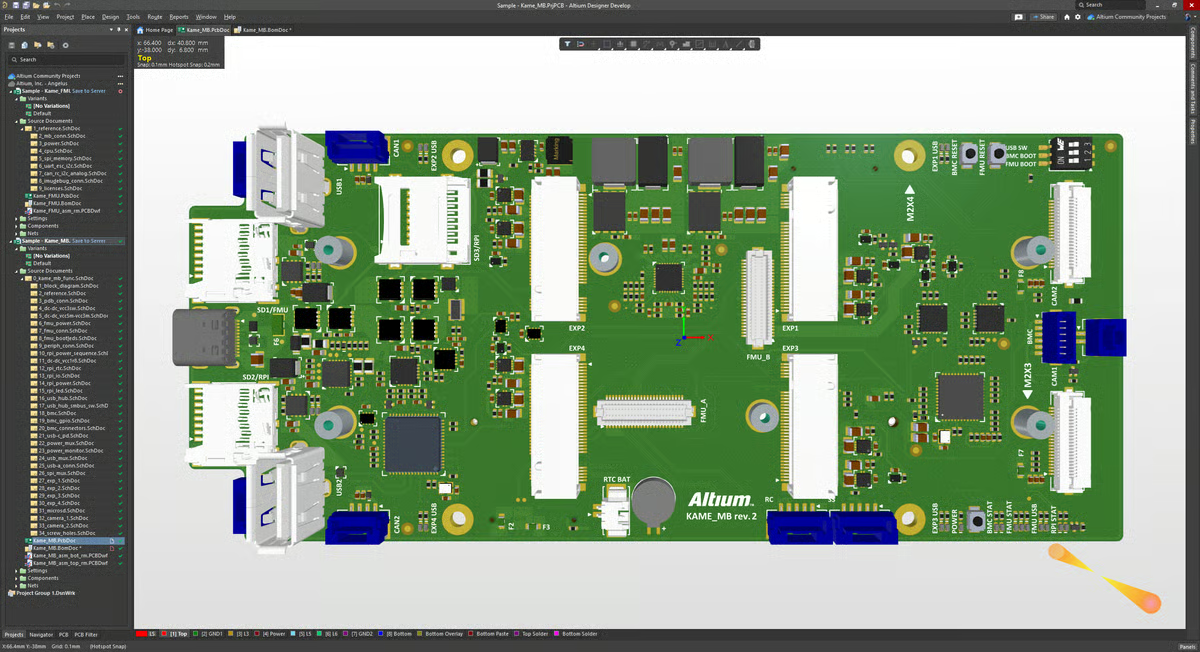
Altium Designer offers a unified platform that integrates different design tools, including schematic capture, layout routing, documentation, and simulation, into one environment. What I appreciate most is the ability to seamlessly move between these stages. For example, once someone creates the schematic diagram, they can easily transition to the layout-routing phase, adjusting the design while visualizing the final product.
A feature that really impressed me is design for manufacturing (DFM). This ensures that designs are not only functional but also easy to produce. The DFM tools help identify potential issues early in the process, reducing errors and saving time during the production phase. Teams I worked with mentioned that it was reassuring for them to know that their design is optimized for manufacturing before moving on to actual fabrication.
With the 3D flex-rigid design, I observed that teams could visualize how the different layers of a PCB interacted, including both flexible and rigid parts. This was especially useful when working with more complex, multi-layered designs. I can see how seeing how each component interacts in 3D can give manufacturers better insight and help them make more informed decisions while routing the layout.
Its extensive component library offers a vast selection of parts, components, and templates, allowing teams to quickly find what they need. This feature reduces the need to manually design components from scratch, and teams can use pre-validated parts that help minimize errors. I observed how the wide selection makes the process faster and more reliable, which is always a plus. According to G2 Data, 83% users love its component libraries.
The biggest aspect I noticed relates to system requirements. Altium Designer performs exceptionally well on high-end machines, but it does require substantial memory and processing power. From what I gathered in G2 reviews, on less powerful computers, there can be some slowdowns with larger, more complex projects. Even so, the software remains very capable for detailed PCB design.
Another area to note is adding footprints to devices. While Altium offers an extensive library, finding the right footprint can involve navigating multiple libraries. Linking the footprint to the schematic symbol isn’t always immediately intuitive, and verifying accuracy can take a few extra steps. Despite these minor inconveniences, the system still allows precise and reliable component placement once familiar with the workflow.
I also gathered from G2 reviews that the learning curve can be steep for beginners. Altium Designer is packed with features, which is a huge advantage for experienced users, though it may take some time to get comfortable with all the tools. Once you’re familiar, the platform’s depth and flexibility really shine, making it a powerful choice for professional PCB design.
"Altium Designer provides everything needed for design and layout in a single tool, eliminating the need for additional purchases. It integrates seamlessly with large-part databases, offering pricing, availability, and efficient manufacturing BOM generation. The built-in SPICE tool supports analog simulation, and its layout features include matched length routing, controlled impedance, differential pairs, and both guided manual and auto-routing, which save significant time once mastered. The integration of 3D mechanical models into designs and outputs for mechanical use is incredibly useful. Overall, Altium Designer is the best electronic design tool I’ve ever used."
- Altium Designer Review, Tim T.
"One area for improvement is adding more features to the "Manufacturer Part Search." Additionally, navigating the software without a mouse can be challenging, especially when using a laptop. Right-clicking and dragging on a trackpad can be frustrating, though that’s partly due to the laptop design. Another suggestion relates to defining board size; for instance, when I needed a board that was exactly 50mm x 50mm, it was hard to draw precise lines. I ended up setting the grid size to 1mm and estimating the dimensions. It would be helpful to have a feature that displays the length of line drawings or the dimensions of the shapes being created."
- Altium Designer Review, Trevor M.
Optimize your PCB production process with advanced manufacturing software.
One of Altium 365's standout features is its real-time collaboration capabilities. From many G2 reviews, I observe that it has helped many circuit teams work on the same designs simultaneously. Whether reviewing schematics or making PCB layout adjustments, it ensured everyone was on the same page. The platform’s version control system ensures that every change is tracked, which allows teams to view revision histories or roll back to previous versions with ease.
It has highly efficient project management tools that have made handling complex designs much easier, especially when working on intricate designs. I found the process of creating and modifying components to be both intuitive and powerful, allowing for detailed work without feeling overwhelming. I can see how this flexibility would be a huge asset for teams, enabling them to manage large-scale projects with ease.
I’ve also gathered from G2 reviews how beginners enjoyed working with the PCB layout editor. It’s incredibly customizable, which allows teams to make adjustments to designs quickly and seamlessly. I really appreciated the ability to effortlessly transition between schematic and PCB. It could save teams a lot of time, as they can quickly modify and export designs. For teams that need to integrate these changes into their larger platform-based projects, I believe that this feature would make the entire process much more efficient.
The 3D visualization feature was another area where Altium 365 impressed me. I could visualize how components fit on the board with ease, especially in tight spaces. The software’s support for .step 3D bodies made it straightforward to see how everything would fit together. What stood out was the 3D rendering speed – even when working with complex components, they rendered quickly without any noticeable lag. I found the "snap points" feature particularly useful, as it helped PCB teams position even the most awkward 3D bodies with great precision.
Lastly, the draftsman tool has been an absolute highlight. Generating high-quality assembly drawings was a breeze with just a few clicks. This tool allowed G2 users to create detailed and visually appealing drawings, which I could imagine would be very beneficial for manufacturing teams that need clear documentation for assembly.

However, despite these positive experiences, I noticed a few areas where PCB routing rules could be improved. Setting them up sometimes required a bit of programming knowledge, which might be tricky for beginners. A more user-friendly interface for configuring these rules would make the process smoother; however, once familiar with the rules system, it provides precise control over design constraints.
Another aspect is the design rule system. Some custom queries, like setting up rules to ignore interfering components, didn’t always behave consistently. For instance, a "component clearance" rule might not always ignore collisions. While this has been reported by several G2 users, the system still allows complex rules to be applied effectively once properly configured.
I also observed that track length calculation could occasionally be inconsistent. Certain small segments on specific layers were sometimes ignored, which could affect impedance-controlled designs. Even so, the platform generally allows accurate track management for most standard layouts.
Lastly, the Bill of Materials (BOM) feature can take a bit longer to generate and requires updating after schematic changes. While this adds some extra steps, it ensures that the BOM remains accurate and reflects all design modifications, which is crucial for precise manufacturing and assembly.
"What I love most about Altium 365 is how effortlessly it enables cloud-based collaboration, making it ideal for real-time PCB design projects, especially for international teams. Its seamless integration with Altium Designer and the ability to access designs from anywhere make it my go-to tool, one I use almost daily. For those using version control tools like Git, the centralized library management and reusable design options significantly speed up development. The intuitive interface becomes easy to navigate with some initial exploration, making it practical for nearly any PCB project. Plus, the growing community support is invaluable."
- Altium 365 Review, Angel O.
"The software can be slow to start and access files, especially over a network. Some default settings, like the connection matrix, generate unnecessary warnings that make it harder to identify real issues. The Bill of Materials feature takes time to generate and requires updates when changes are made to the schematic. Additionally, the software slows down with larger designs, and while it integrates well with third-party components, occasional issues with mismatched footprints or symbol standards can arise."
- Altium 365 Review, Hemant A.
One of the biggest strengths I noticed about PAD Professional is its ability to handle complex PCB layouts. This feature was particularly useful when teams I worked with created intricate designs requiring precise control.
The interactive features, especially the auto-routing options, truly stood out to me. They significantly sped up the layout process, and teams could visually track the routing as it progressed, making the entire process smoother and more efficient.
Another standout aspect is the extensive documentation. From many reviews, I gathered that G2 users relied heavily on the documentation at the beginning, and it didn't disappoint. It covered everything from basic functionality to more advanced options, helping teams quickly understand features that could have otherwise been challenging to figure out.
I also appreciated the schematic part view, which lets you rotate components at different angles. This was a surprisingly helpful feature, making it easier to visualize and work with frequently used components, especially those that need specific orientations. According to G2 Data, 82% users praise its schematic editor.
One of the most impressive integrations I came across was the link to HyperLynx for signal integrity or power Integrity simulations. I observed how effortlessly it could perform detailed simulations, and the seamless integration really enhanced the tool’s capabilities.

The flexible design constraint system allowed users to easily define specific design rules, adding precision to designs and ensuring compliance with manufacturing requirements. I did notice, however, that G2 users mentioned this feature could be even more powerful if paired with improved usability for template creation, though it still provides strong control over design constraints.
I also found that the initial setup could feel a bit overwhelming. The tool offers many features, and getting it up and running isn’t as simple as some users might hope. A more streamlined setup process could help, but once configured, the platform functions effectively.
Many users noted that while the GUI works, the interface feels somewhat outdated compared to modern PCB design tools. After analyzing multiple G2 reviews, I observed that while the tool is fully functional, a more intuitive and visually engaging interface could enhance navigation, though the core functionality remains solid.
Another point is dashboard performance. For some designs, computing and processing analysis can take longer than expected. Even for simple projects, this wait can feel noticeable, though it doesn’t affect the accuracy or overall usefulness of the analysis.
I also discovered, from G2 reviews, that constraint manager template creation and reuse could be more intuitive. While the system is flexible, creating and reusing templates can feel cumbersome. Improving this workflow would enhance user experience, but the existing system still allows precise constraint management.
Lastly, support for importing legacy designs could be more robust. Importing older designs may take extra time, which could be a minor pain point for users transitioning from other tools. Even so, the platform provides sufficient functionality to handle legacy projects effectively once imported.
"It's very helpful for backend design and highly reliable with excellent accuracy. The user interface is supportive and professional, making it easy to use repeatedly for designing and analyzing PCB fabrication. Integration is simple, and the customer support from Mentor Graphics is outstanding. Overall, it's easy to implement."
- PADS Professional Review, Subhadeep P.
"One downside of using PADS Professional is that it takes a significant amount of time to process and compute analyses, even for something as simple as the dashboard, which can be quite frustrating."
- PADS Professional Review, Souvik G.
Streamline your PCB design process by collaborating with version control software.
I recently explored Allegro X PCB Designer, and I found it exceptional for creating CPU motherboards and working with high-density interconnect (HDI) PCB designs.
Its ability to develop compact, space-efficient electronics while maintaining advanced functionality is impressive. From G2 user reviews, I observed that the tool makes it possible to pack intricate components into smaller spaces, a feature that really stood out to me and felt like a significant advantage for modern electronics design.
One of my favorite features is the error correction system for schematic design. With its three-step process, it made ensuring schematic accuracy feel intuitive and simple for professionals. I noticed across multiple reviews that it flagged errors early, corrected them logically, and validated the results systematically, streamlining the design process and minimizing potential mistakes.
I also appreciated the pre-analysis and post-analysis capabilities, which allowed users to catch and resolve issues both before and after the design phase, making the entire workflow more efficient and reliable.
I was also impressed by Allegro’s flexible workspace, This adaptability was a huge plus for PCB management teams, as it made staying organized and productive much easier. Aligning the tool’s setup with design habits felt like a great way to improve efficiency and comfort.

The flexible design constraint system allowed users to easily define specific design rules, adding precision to designs and ensuring compliance with manufacturing requirements. I did notice, however, that G2 users mentioned this feature could be even more powerful if paired with improved usability for template creation, though it still provides strong control over design constraints.
I also found that the initial setup could feel a bit overwhelming. The tool offers many features, and getting it up and running isn’t as simple as some users might hope. A more streamlined setup process could help, but once configured, the platform functions effectively.
Many users noted that while the GUI works, the interface feels somewhat outdated compared to modern PCB design tools. After analyzing multiple G2 reviews, I observed that while the tool is fully functional, a more intuitive and visually engaging interface could enhance navigation, though the core functionality remains solid.
Another point is dashboard performance. For some designs, computing and processing analysis can take longer than expected. Even for simple projects, this wait can feel noticeable, though it doesn’t affect the accuracy or overall usefulness of the analysis.
I also discovered, from G2 reviews, that constraint manager template creation and reuse could be more intuitive. While the system is flexible, creating and reusing templates can feel cumbersome. Improving this workflow would enhance user experience, but the existing system still allows precise constraint management.
Lastly, support for importing legacy designs could be more robust. Importing older designs may take extra time, which could be a minor pain point for users transitioning from other tools. Even so, the platform provides sufficient functionality to handle legacy projects effectively once imported.
"This user-friendly software makes both pre-analysis and post-analysis easy to perform. It includes integrated circuit (IC) input/output buffer information Specification (IBIS) models for signal integrity and power integrity analysis. The software offers various types of analysis, such as electrical analysis, thermal analysis, and eye diagram analysis. It also synchronizes easily with capture and provides floor-planning features. Additionally, auto-placement and auto-routing are available, making the design process more efficient."
- Allegro X PCB Designer Review, Nikhil K.
"The software needs to be backward compatible with older revisions. It requires switching between different toolsets, and the entire workflow isn't easily integrated. STEP export files don't work well with SolidWorks, and managing libraries and variants can be difficult."
- Allegro X PCB Designer Review, Vijay P.
During my evaluation of Autodesk Fusion, one aspect that stood out to me was the 3D design and modeling tools. These tools are incredibly powerful and allow for the creation of simple parts and complex structures.
Users often commend manufacturing integration. Fusion enables designs to be taken directly from concept to production, streamlining the process. Instead of switching between multiple platforms for design and manufacturing, everything is consolidated in one place. In fact, according to G2 Data, 86% users appreciate its catalog integration capacity. For manufacturing teams, this feature is invaluable as it reduces the chances of errors and ensures all parts of the process are streamlined.
One of the most innovative features I evaluated was generative design. This tool allowed G2 users to input design goals and constraints, and Fusion then generated multiple design options that met those criteria. For manufacturing teams, this can be incredibly useful for exploring new design possibilities and optimizing efficiency, as the software suggests design alternatives that might not have been considered otherwise.

However, I found that assemblies in Fusion can be challenging to manage, particularly for larger designs. Organizing and navigating through different parts can feel cumbersome, and locating specific components quickly may take extra effort. Even so, once familiar with the assembly workflow, the platform allows precise control over complex designs.
Another area I noticed is 2D drawing tools. Fusion provides basic functionality for creating 2D drawings from 3D models, but many G2 users mention that options for intricate 2D designs are limited. For advanced drawings, exporting to AutoCAD is sometimes necessary. Despite this, the existing 2D tools handle standard designs effectively and support manufacturing needs for most projects.
Finally, I observed some considerations with file conversion. While Fusion supports a wide range of formats, certain intricate details and geometries may not always transfer perfectly when importing into other software. Even so, the platform maintains high fidelity for most designs, and these minor conversion issues can usually be managed with careful checks.
"I like using Fusion as a great 3D CAD program for creating parts or simple assembly designs. The layout and functions feel mostly familiar, and the small differences from other CAD software I've used were easy to adjust to. Fusion also seems designed with collaboration in mind, making it easier to work together on designs (although I haven't used this feature much, I can see its value). One of Fusion's biggest advantages is its price. I had trouble convincing management to pay for 3D CAD software due to the high costs, but Fusion was much easier to justify, costing around 10% of what Inventor or SolidWorks would."
- Autodesk Fusion Review, Justin B.
"Two aspects of Autodesk Fusion 360 that I find less favorable are its reliance on an internet connection and its CAD file compatibility. While being cloud-based offers significant benefits, features like real-time collaboration and automatic saving can be challenging in areas with limited connectivity. Additionally, although Fusion 360 supports many file formats, the conversion process during export is often limited, leading to the loss of details or geometries when importing files into other software."
- Autodesk Fusion Review, Juan M.
Unlock your design potential with powerful prototyping software. Start building and testing your prototypes today to bring your ideas to life!
After evaluating Altium CircuitMaker, I can confidently say that this tool has a lot to offer, particularly for those working on circuit design.
One of the features I appreciated the most was the cloud integration. This allowed teams to store all designs securely in the cloud, making them accessible from anywhere. It was incredibly convenient, as they didn't have to worry about losing their work or managing storage space on my local machine.
Additionally, the ability to collaborate easily with others I think is a huge plus. Whether you're working remotely or on a team-based project, this cloud feature makes it seamless to share and work on designs together.
I also noticed that many users mention the Fusion 360 plugin made a significant difference. This plugin allowed teams to effortlessly bridge the gap between electronic and mechanical designs. They can work on circuit design in CircuitMaker and then seamlessly transition to Fusion 360 to refine the mechanical components, or vice versa. This fluid integration between the two platforms saved them hours of reworking and resolving alignment issues, ensuring that their electronic and mechanical designs aligned perfectly.
I also gathered that the 3D technology for visualizing schematics was a game-changer. Seeing designs in 3D helped them understand how the circuits would interact once they were physically built. It provided a much clearer picture than the traditional 2D view.
I also really appreciated the ability to easily assign properties to components. Adding comments or specific attributes to parts helped teams stay organized and keep track of changes throughout the design process. It was particularly useful for leaving reminders about specific design decisions or particular parts, ensuring that nothing was overlooked.

However, I noticed a few considerations with simulator accuracy. While the simulator works well for basic circuits, some G2 reviewers noted that it may not always accurately reflect real-world behavior for more complex designs. Even so, the platform provides reliable simulation for most standard projects, and these occasional inaccuracies are generally limited to highly intricate circuits.
While cloud integration works smoothly and enables easy collaboration, I observed that projects cannot be saved offline. This means an internet connection is required, which could be inconvenient in areas with poor connectivity. Despite this, the cloud-based workflow offers seamless access and version control for teams.
I also found that community sharing is heavily relied upon. While many users enjoy the collaborative aspect, some prefer more control over their own projects. Even so, the shared resources can be a valuable starting point and inspiration for many designs.
Lastly, I noticed that Linux and macOS support is limited. CircuitMaker is primarily designed for Windows, so non-Windows users need a virtual machine to run the software. While this adds an extra step, the platform functions well within the virtual environment, allowing users outside Windows to still access its core features.
"CircuitMaker is a great tool for designing and operating electrical circuits. Its intuitive interface allows you to quickly draw, modify, and combine layouts with ease. It's a precise tool that makes it simple to understand the theoretical aspects of electrical circuits. With the program's libraries, you can create impressive projects, and finding an element is made easy through a nested structure within subfamilies. This tool includes all the necessary features to be used professionally in your company or organization."
- Altium CircuitMaker Review, James Michael W.
"CircuitMaker enforces cloud saving and allows only two private projects, which can be limiting. The community component library is unmoderated, containing many unusable footprints (though it's recommended to create your own, as the component wizard makes it easy). The software can be somewhat unstable, so saving frequently is important. Additionally, the keyboard shortcuts differ from those in Altium Designer, which may take some time to adjust to."
- Altium CircuitMaker Review, Alberto V.
One feature of Autodesk EAGLE that stood out to me almost immediately was the built-in user language programs (ULP). Many users mention how it helps them save time by automating repetitive processes, which is helpful when working on multiple designs or making frequent adjustments.
The autoroute function is another tool that simplifies the design process. In a manufacturing context, where time is critical, the ability to quickly route paths with minimal manual effort was invaluable. I observed that it allowed users to generate quick prototypes, focusing more on refining the core design rather than dealing with routing issues.
After reading numerous reviews, I gathered that the tool reportedly works smoothly for schematic capture, which is crucial in manufacturing for ensuring accuracy. It helped spot potential issues early in PCB workflows, reducing the likelihood of errors during production.

On the library management side, Autodesk EAGLE impressed me with its extensive selection of pre-loaded CAD packages. This meant less time spent searching for components, allowing for faster assembly and prototyping in manufacturing.
One area I noticed with the 3D visualizer is that, while functional, it doesn’t always provide the level of accuracy some users expect when visualizing a PCB’s final look. In manufacturing, precision is crucial to ensure a proper fit, but even with this limitation, the visualizer still provides a good overall representation of the board layout.
I also observed some reports regarding the net listing feature. For complex power PCBs, it doesn’t always behave as expected, which can lead to minor delays in design verification. Despite this, the feature generally helps maintain proper electrical connections across most standard projects.
Another consideration is the layer restriction in the downloaded version of EAGLE, which limits designs to two layers. This can be challenging for multi-layer boards, but the limitation is mainly relevant for high-density designs. Teams working on simpler boards will still find the platform very effective.
Lastly, I noticed feedback about routing intelligence. Currently, EAGLE uses standard routing paths, and some users suggest that AI-based routing could improve efficiency. Even so, the existing routing tools allow users to create reliable, precise designs, and enhancements like AI integration would be a welcome improvement.
"The CoA template was customized to meet our needs, including all essential client and sample details, along with a table displaying analytes and their observed values. Each table cell was designed to capture values based on specific test types. The CloudLIMS team collaborated closely with us to ensure the template matched our expectations. They automated calculations and applied built-in logic and complex algorithms to make this happen."
- Autodesk EAGLE Review, Ronel C.
"The system’s session timeout is quite restrictive, as the platform prompts session expiration after a short period. It would be helpful if there were an option to extend the session duration, giving users more flexibility to complete tasks without the concern of losing their progress."
- Autodesk EAGLE Review, Aryan K.

To design a PCB, start by creating a schematic diagram that outlines the circuit components and their connections. Then, use PCB design software to convert the schematic into a PCB layout, placing components and routing the traces. After completing the layout, generate the necessary files for manufacturing, such as Gerber files, and ensure design rules and electrical constraints are met.
Yes, some PCB design apps are available for mobile devices; however, they tend to have fewer features compared to their desktop counterparts. These mobile apps are suitable for basic design tasks and simple projects, but for more complex designs that require advanced functionality, desktop software is recommended due to its greater precision and comprehensive toolsets
You can learn PCB design through online courses, tutorials, and books that cover electronics and circuit design. Begin by understanding basic concepts, such as circuit schematics and component placement, and then practice using free PCB design software. Start with simple circuits to build your skills before progressing to more complex projects. Engaging with online forums or communities can provide valuable feedback and guidance, helping you gain confidence before using advanced design tools.
Choosing the right PCB layout design depends on factors like the project’s size, complexity, and required functionality. Consider the number of layers, the type of components used, thermal management, and signal integrity. For high-speed circuits, pay special attention to routing and grounding. Additionally, ensure the layout meets any industry-specific requirements (e.g., automotive or medical standards).
Most high-quality PCB design software tools are paid, but many offer free trials to help you get started. Altium Designer, for example, is widely regarded as one of the best tools in the industry, offering powerful features for complex designs. Its free trial can be a good starting point. Explore more free PCB design software that offers basic features, which can be useful for simpler projects or beginners.
Choosing the right PCB design software can be a game-changer for your projects. When evaluating these tools, it’s essential to consider factors like usability, performance, and features that best align with your specific needs, whether that’s handling complex designs, improving signal integrity, or ensuring smooth collaboration.
Based on my evaluation and user feedback, I’ve outlined the top tools that offer the best combination of efficiency, flexibility, and power. The best tool is the one that works for you and helps you bring your PCB designs to life without any hiccups.
Don’t be afraid to dive in, experiment with different options, and see what clicks. Remember, even the most sophisticated software can’t help if you don’t press the right buttons (unless you have a “design wizard” on your team, in which case, please share their contact information with me).
Reduce errors by using simulation and test suites before moving your PCB design to production.
.png)

We have come a long way from sketching on notepads.
 by Harshita Tewari

3D printing is awesome, until your software turns it into a nightmare.
 by Washija Kazim

There’s something to be said about seeing an idea or a design come to life.
 by Mara Calvello